
allied
academies
Materials-Metals 2017
Page 15
November 16-17, 2017 Paris, France
13
th
Annual Conference on
Materials Science, Metal and Manufacturing
Journal of Materials Science and Nanotechnology
Volume 1 Issue 2
Se-Young Jeong, Mater Sci Nanotechnol 2017, 1:2
Fabrication of wafer-scale grain boundary free Cu
single crystal film and copper oxide film by sputtering
method and its application
Se-Young Jeong
Pusan National University, Republic of Korea
C
opper thin films have been widely used as electrodes and
interconnection wires in integrated electronic circuits,
and more recently as substrates for the synthesis of graphene.
However, the ultra-high vacuum processes required for high-
quality Cu film fabrication, such as molecular beam epitaxy
(MBE), restricts mass production with low cost. In this work,
we demonstrated high-quality Cu thin films using a single-
crystal Cu target and sputtering technique; the resulting film
quality was comparable to that produced using MBE, even under
unfavorable conditions for pure Cu film growth. The Cu thin film
was epitaxially grown on an Al
2
O
3
(0001) substrate, and had high
crystalline orientation along the (111) direction. Despite the 10-
3
Pa vacuum conditions, the resulting thin film was oxygen free
due to the high chemical stability of the sputtered specimen from
a single-crystal target; moreover, the deposited film had > 5 X
higher adhesion force than that produced using a polycrystalline
target. We applied the technique fabricating the single crystal
thin film to the flexible transparent conducting electrodes, where
a micromesh/nanomesh structure was fabricated on a polyimide
substrate using UV lithography and wet etching. We also
succeeded to fabricate a wafer-scale graphene in the formation
of artificial single crystalline AB-BLG via aligned transfer of two
single-crystalline monolayers. Such single crystal copper film
was realized not only on the sapphire substrate, but also on the
PI, PET, and PC, which enabled to apply in the region of flexible
devices, metamaterial and of surface plasmonics. The important
advantage of this single crystal copper film is due to the natural
oxide layer with a thickness of around 2nm, which protects
further oxidation, so that the copper layer maintains clean even
for 2-3 years without any capping layer. Well-defined conditions
enabled the copper film to convert to Cu
2
O or CuO partially
or totally, which are transparent and p-type semiconductor. In
the partially oxidized case, the copper layer left beneath Cu
2
O
or CuO could be used as electrode. The color of the film varies
between transparent gold and opaque metallic scarlet depending
on the ratio of metal and oxides. Thanks to the grain free copper
thin film, the copper oxides also maintain high crystallinity.
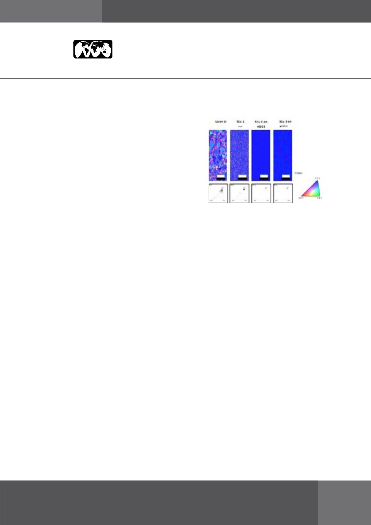
Figure 1:
The EBSD images of commercial copper film (Cu on
Si), single crystal copper film under unoptimized conditions
SCu
1
and SCu
2
) and single crystal copper film under optimized
condition (SCu
3
)
Recent Publications
• Nguyen VL, Perello DJ, Lee S, Nai CT, Shin BG, Kim JG,
Park HY, Jeong HY, Zhao J, Vu QA, Lee SH, Loh KP, Jeong
SY and Lee YH (2016) Wafer-scale single-crystalline AB-
stacked bilayer graphtene. Advanced Materials, 28: 8177-
8183.
• Lee S, Wi HS, Jo W, Cho YC, Lee HH, Jeong SY, Kim YI, Lee
GW (2016) Multiple pathways of crystal nucleation in an
extremely supersaturated aqueous potassium dihydrogen
phosphate (KDP) solution droplet, PNAS 113: 13618-13623.
• Kim WK, Lee S, Lee DH, Park IH, Bae JS, Lee TW, Kim
JY, Park JH, Cho YC, Cho CR, Jeong SY (2015) Cu Mesh
for Flexible Transparent Conductive Electrodes. Sci. Rep. 5:
10715-10722
• Kim JY, Oh MW, Lee S, Cho YC, Yoon JH, Lee GW, Cho CR,
Park CH and Jeong SY (2014) Abnormal Drop in Electrical
Resistivity after Impurity Doping of Single Crystal Ag. Sci.
Rep. 4: 05450-05454
• Phamcong D, Choi JH, Yun J. Bandarenka A. Kim J. Braun
P. Jeong SY, Cho CR (2017) Synergistically Enhanced
Electrochemical Performance of Hierarchical MoS2/
TiNb2O7 Hetero-Nanostructures as Anode Materials for
Li-Ion Batteries. ACS Nano 11: 1026-103.


