Research Article - Biomedical Research (2018) Computational Life Sciences and Smarter Technological Advancement: Edition: II
Battery less thermo electric energy harvesting generator for implantable medical electronic devices
1Assistant Professor (Slg), Kongu Engineering College, India
2PG Scholar, Kongu Engineering College, India
Accepted date: June 16, 2017
DOI: 10.4066/biomedicalresearch.29-17-1396
Visit for more related articles at Biomedical ResearchAbstract
Pacemakers are used to treat slow heart rate diseases like bradycardia. The main problem about pacemakers are the lifetime and size of the batteries. As the capacity of the batteries is limited, replacing these batteries is difficult since it requires surgical procedures and also 60% of the volume of a pacemaker is taken up by its batteries. Eliminating these batteries effectively reduces the dimensions of the pacemaker. Thermoelectric Generators (TEG) can be used to power up the pacemakers without limiting the capacity with effective reduction in the dimension. The pellicani charge pump has been designed to pump the minimum voltage from the TEG to the voltage upto 1.2 V with minimum number of stages.
Keywords
Pacemaker, Bradycardia
Introduction
The normal resting heart rate is 60 to 100 BPM for adults. Bradycardia also known as bradyarrhythmia is a slow heart rate defined as a heart rate of under 60 Beats Per Minute (BPM) in adults. A pacemaker is implanted to treat slow heart beating. A pacemaker is a small device implanted just below the collarbone.. The signals from the Pacemakers are carried along thin insulated wires to the heart muscle to begin the contractions that causes the heartbeat. The main problem about pacemakers is their batteries because the capacity of the batteries is limited. One should undergo a surgical procedure to replace the battery of the pacemaker after a period of five years. About 60% of the volume of a pacemaker is taken up by its batteries. Eliminating these batteries effectively reduces the dimensions of the pacemaker. Thermo electric generators are used to harvest the waste heat generated from our body which is about 50 mV. This small voltage has to be boosted up to 2.5 V which is the necessary operating voltage of the Pacemakers by using the Voltage multiplier circuit. Upto now the voltage multiplier i.e., the boost converters are started by the load capacitor, mechanical switch and 95 mV start-up voltage.
Alhawari et al. [1] proposed an Efficient Thermal Energy Harvesting IC (EHIC) that supports a battery-less μ Watt system-on-chips. The EHIC consists of an inductor-based DCDC converter that boosts a low input voltage to a suitable output voltage level. Further, a switched capacitor buck converter is utilized to regulate the boost converter output voltage and to support multiple output voltage levels, namely 0.6 V, 0.8 V and 1 V. In low energy mode and to enhance the efficiency, the EHIC is capable of bypassing the switched capacitor so that the load is driven directly from the boost converter. Siouane et al. [2] presented a thermoelectric generator under constant heat flow conditions. Thermoelectric generators can be used under constant temperature gradient or constant heat flow conditions.
A simulator-friendly circuit model for a magnetic core is used to design and demonstrate several power electronic circuit solutions for harvesting energy was designed by Moon et al. [3]. The circuit model had excellent accuracy to represent the core regardless of the level of saturation. A design of boost converter Hybrid Micro Energy Harvester (HMEH) using thermal and vibration of human body for biomedical application was modelled by Asni et al. [4]. Thermal converter converts temperature differences directly into electrical energy. While vibration is based on human movement like walking and shaking body that is able to generate an AC voltage. Having two sources overcome the limitation caused by a 5 single source harvester and improves system functionality. The inputs are set to 0.2 V, 0.3 V and 0.5 V to represent thermal, vibration and combination of thermal and vibration (hybrid) respectively. A rectifier is designed to convert vibration input from AC to DC voltages. The proposed boost converter is used to step-up the small input voltage from thermal and vibration at 2 kHz. Das et al. [5] proposed a start-up circuit based upon output voltage feedback for thermal energy harvesting. The feedback loop consisting of an output load, a boost converter core, a charge-pump-based doubler and a CMOS inverter switch to track the output voltage and generate a reset signal to kick-start the boost converter [6-10]. The proposed start-up circuit shows a remarkably improved start-up time of 35 μs at the input voltage of 290 mV. The start-up circuit is automatically disabled after the boost converter reaches steady-state.
Proposed Work
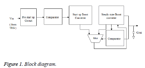
Typical Thermoelectric Generator (TEG) is the main component in the thermoelectric energy harvesting chain which uses Seebeck effect to convert heat into electrical energy. The voltage multiplier circuit is a boost converter based on a Constant Charge Time (CCT) structure. The output voltage of a TEG is applied to the input of this system. The Prestart up circuit used in the system comprises of low voltage low power oscillator and the charge pump. An ultralow-voltage low-power oscillator generates the required clock phases for a Charge Pump (CP) system. The output voltage of the TEG is applied to the input of CP. Consequently, CP begins to charge a small internal capacitor placed at its output and the capacitor voltage begins to rise. When the capacitor voltage reaches a predefined value, the output of the comparator sets. This enables the Start-Up Boost Converter (SUBC) to work. The SUBC provides the required clock phases for the Steady-State Boost Converter (SSBC), while the SSBC output voltage (VOUT) does not reach a preset value. When this is achieved, the output of the comparator 2 sets and the normal operation of the system begin. In this mode, the SSBC itself generates its clock phases. A multiplexer is used to select the source of the required phases for the SSBC based on the comparator voltage. In normal operation, the SSBC no longer requires the prestartup CP and SUBC, so it can continue to work on its own. It is designed so that VOUT becomes a regulated output voltage.
The Figure 1 shows the block diagram of proposed method. The thermo electric generators are used to provide a low voltage of 50 mV. This low voltage is used as a supply voltage to the ring oscillator and the charge pump. The ring oscillator provides the clock pulses for the charge pump to work on two phases. This 50 mV is converted to 1.2 V by the charge pump (Figure 2).
Prestartup Charge Pump Structure
Low-voltage low-power oscillator
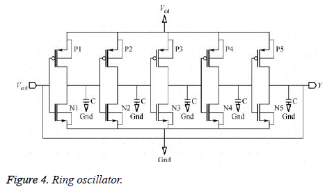
The output voltage of a TEG is very low. It is not sufficient for conventional oscillators to work properly. Among different types of oscillators, ring oscillators consume less power. A ring oscillator comprises an odd number of inverters placed in a loop. Figure 3 shows the ring oscillator with five stages with output buffer.
Figure 3 shows the structure of the proposed low-voltage oscillator with its output buffer. Ring oscillator consumes less power when compared to other types of oscillators. The charge pump requires the high frequency clock signals to charge the output capacitor. To design the highest frequency oscillator, the oscillator is to be designed with minimum number of stages. In addition, to minimize the power consumption, minimum sized inverters are used. The output buffer consists of a chain of inverters.
Low-voltage high-efficiency charge pump
Charge pump is one type of DC-DC converter that is often used to produce high DC voltage from a given supply. The simple structure of charge pump is used in applications such as read/write operation of EEPROM and MEMS MIC, which have relatively low load current with moderate ripple requirements. The significant characteristics of the Charge pumps are output voltage, input voltage, internal capacitor values, current, frequency of the oscillator and output voltage ripple. The conventional Charge Pump (CP) which is used to pump up the input voltage upto the optimum voltage required for driving the Pacemakers. The Charge pump has to be designed with minimum number of stages and low power dissipation to obtain the optimum voltage level.
Digital control circuit
The digital control circuit is used in the system to control the Boost converters. Based on the output voltage of the comparators the boost converters will start its operation in both the start-up mode and the steady state mode. The output voltage from the comparator 1 enables the start-up boost conversion operation and the output voltage from the comparator 2 enables the Steady state boost converter. The digital control circuit also contains the multiplexer which is used to select the output voltage of the steady state and the start-up boost converters.
Boost converters
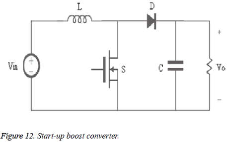
Start-up boost converter: The start-up boost converter is a dc power supply that is small, lightweight and highly efficient, and uses a semiconductor switching element. It is comprised of
(i) Switching power supply unit which, can turn ON/OFF switching elements that can be turned ON/OFF at high frequency to convert a dc input voltage VIN into a dc output voltage VOUT.
(ii) A control unit, which is used to control the ON/OFF operation of the switching element of switching power supply unit.
Results and Discussion
Ring oscillator
A ring oscillator is a circuit which consists of an odd number of inverter stages, where the output of each stage of the ring oscillator is given to the input of next stage and output of final stage is then fed to its input. The basic element in ring oscillator is an inverter cell. The cell consists of complementary pairs of pMOS and nMOS. In a ring oscillator, the gain stages are connected in a loop that output from the last stage is given to the input of first stage. The ring oscillators have been designed using Synopsis custom designer tool in 32 nm CMOS technology.
Figure 4 shows the designed ring oscillator using 32 nm technology. The Ring oscillator is used to provide the clock cycles for the pre charge up circuit. The input voltage given to the ring oscillator is 40 mV which is produced by the thermal energy harvesters. The ring oscillator is designed with minimum number of stages to provide the clock cycles because the higher number of stages increases the power dissipation and the number of transistors.
Output waveform of ring oscillator
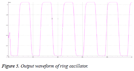
The Figure 5 shows the output waveform of the designed ring oscillator in 32 nm technology. This designed ring oscillator is used to start the charge pump process. The Oscillator is designed with minimum number of stages to get the maximum frequency. The ring oscillator provides the clock cycles to the CP continuously to pump up the input voltage.
The Table 1 shows the obtained parameters from the ring oscillator. The ring oscillator is designed with the high operating frequency of 564 MHz. The important performance parameters like frequency and power consumption were measured for the ring oscillator.
| Parameter | Value |
|---|---|
| Time | 1.77 ns |
| Frequency | 564 MHz |
| Power consumption | 490 nW |
Table 1. Parameters obtained.
Charge pump
A charge pump circuit provides a voltage that is higher than the voltage of the input power supply or a voltage of reverse polarity. Increased voltage levels are obtained in a CP as a result of transferring charges to a capacitive load and do not involve amplifiers or transformers. For that reason in semiconductor technology a charge pump is a device of choice where normal range of operating voltages is limited. Charge pump are widely used because they can be implemented on the same chip together with other components of an integrated system.
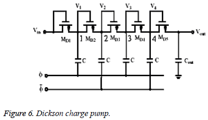
Figure 6 shows the modified Dickson charge pump which is used to pump the input voltage of 40 mV to 1.2 V. The proposed CP was designed for a 32 nm CMOS technology. CP is used to pump the low input voltage to very high output voltage. The modified Dickson charge pump pumps the output voltage from the thermo electric generators to the voltage of 1.2 V.
Output waveform of Dickson charge pump
The Dickson charge pump has the voltage gain which is proportional to the total number of stages in the charge pump. The operation of the charge pump depends on the switching on and off a large number of MOS switches. These MOS switches charge and discharges the capacitors which transfers large amount of energy to the output load. Whenever the load current is reduced large amount of energy is lost.
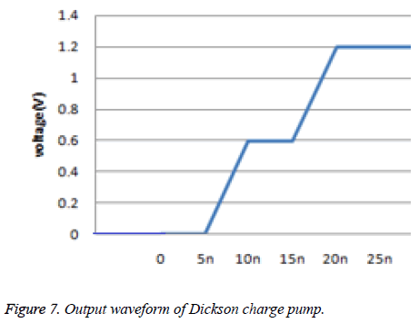
Figure 7 shows the output waveform of Dickson charge pump with output voltage of 1.2 V which can be used for the pacemakers to treat the disease called bradycardia. The number of stages used to design the Dickson charge pump is five which is very high and hence the Pelliconi charge pump is designed to obtain the optimum voltage with minimum number of stages of four.
Pelliconi charge pump
The Pelliconi charge pump has higher output voltage and robustness to the variation of the clock. The body effect is controlled by connecting each devices substrate to its source. In a cascade configuration, each source/substrate has a different voltage, so transistors of the same type in each stage must be in a well isolated from the well of the other stages.
Figure 8 shows the Pelliconi CP designed that can be used to obtain the required voltage level with minimum number of stages when compared to the Dickson CP. Hence the Pelliconi charge pumps are preferred over the Dickson charge pump to obtain the necessary operating voltage required for the effective operation of the Pacemakers used to treat the cardiac diseases like bradycardia.
Output waveform of Pelliconi pump
The designed Pelliconi CP has an advantage over the Dickson charge pump in such a way that the high output voltage is obtained with the minimum number of stages with low power consumption.
Figure 9 shows the output waveform of the Pelliconi charge pump whose output voltage is 1.2 V which can be used to power up the pacemakers. Pacemakers makes uses this 1.2 V to provide the necessary pulses to the walls of the heart to treat the slow heart rate disease called bradycardia.
The Table 2 shows the comparison of the designed Dickson charge pump and the Pelliconi charge pump. The Pelliconi charge pump has better efficiency over the Dickson charge pump with minimum number of stages and minimum power consumption. Thus Pelliconi charge pump is preferred over the Dickson charge pump.
| Parameters | Dickson charge pump [1] | Pelliconi charge pump |
|---|---|---|
| Input voltage | 40 mV | 40 mV |
| Number of stages | 5 | 4 |
| Number of transistors | 100 | 16 |
| Output voltage | 1.2 V | 1.2 V |
| Power consumption | 710 μW | 385 μW |
Table 2. Comparison of the charge pumps.
Folded-cascode comparator with external hysteresis
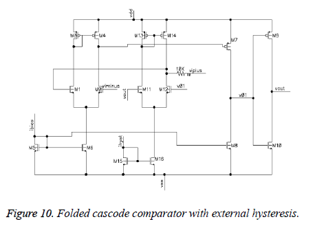
The folded cascode comparator shown in Figure 10 is used to compare the output voltage from the pre start up circuit with the reference voltage. If the output voltage is greater than the reference voltage the start-up boost converter will be enabled to start its boost conversion operation.
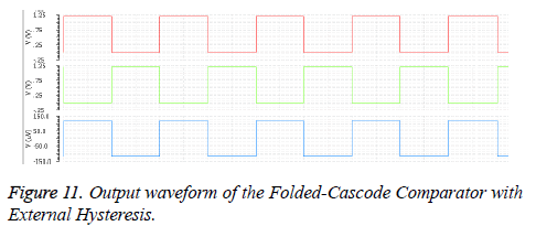
The designed folded cascode comparator has an external hystersis with better performance than the other types of comparators. The output waveform of the folded cascode comparator is shown below (Figure 11).
The output waveform of the folded cascode comparator with external hysteresis shows when the input voltage is greater the reference voltage the output voltage of the comparator will be high else the voltage level of the comparator will be low. This high voltage level of the comparator is used to enable the startup boost converter to start its boost conversion operation.
Start-up boost converter
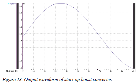
The start-up boost converter shown in Figure 12 gets the input voltage from the Comparator. If the input voltage is high then the boost converter starts its boosting operation. The output voltage of the boost converter is 2.4 V from the input voltage of 1.2 V.
Steady state boost converter
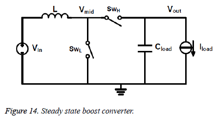
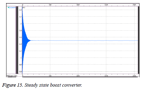
The steady state boost converter shown in Figure 13 is used to provide the steady state output voltages necessary to drive the implantable medical electronic devices such as pacemakers. The steady state boost converters derive its input voltage from the start-up boost converters whose output has to be regulated to a steady voltage.
The capacitor charges and discharges the voltage from the Inductor as shown in the Figure 14. This steady state output from the output capacitor can be applied for the implantable medical electronic devices such as pacemakers.
The peak voltage of 2.4 V has been obtained from the designed steady state boost converter is shown in the Figure 15. This maximum voltage of 2.4 is the sufficient driving voltage of implantable medical devices like pacemakers.
Conclusion
The TEG provides the input voltage for the pacemaker from the temperature difference found between the body and the ambience. Using the FBB technique, a low-voltage oscillator and a low-voltage CP have been designed and simulated which enables the circuit to start up from input voltages as low as 40 mV. The pre charge up circuit for the boost converters has been designed and the parameters are obtained. The ring oscillator with the minimum number of stages has been designed to obtain the maximum frequency of oscillations and the output is fed to the charge pump circuit. The pellicani charge pump pumps the voltage upto 1.2 V. The output voltage of 2.4 V is obtained from the Boost converters with low power dissipation.
References
- Alhawari M, Dima K, Baker M, Hani S, Mohammed I. An efficient thermal energy harvesting and power management for μ Watt wearable BioChips. IEEE International Symposium on Circuits and Systems (ISCAS) 2016; 2258-2261.
- Siouane S, Slavisa J, Philippe P. Equivalent electrical circuit of thermoelectric generators under constant heat flow. IEEE 16th International Conference on In Environment and Electrical Engineering (EEEIC) 2016; 1-6.
- Das A, Gao Y, Kim TTH. An output feedback-based start-up technique with automatic disabling for battery-less energy harvesters. IEEE International Symposium on Circuits and Systems (ISCAS) 2015; 233-236.
- Huleihel Y, Cervera A, Ben-Yaakov S. A high gain DC-DC converter for energy harvesting of thermal waste by thermoelectric generators. IEEE Convention on Electrical and Electronics Engineers in Israel 2012; 1-5.
- Jambek AB, See CP, Hashim U. Analysis of energy harvesters for powering a wireless sensor node device. IEEE International Conference on Semiconductor Electronics (ICSE) 2012; 769-773.
- Leonov V. Thermoelectric energy harvesting of human body heat for wearable sensors. IEEE Sens J 2013; 13: 2284-2291.
- Lim MS, Ali SH, Jahariah S, Islam MS. Modelling of hybrid energy harvester with DC-DC boost converter using arbitary input sources for ultra-low-power micro-devices. IEEE International Conference on Semiconductor Electronics (ICSE) 2014; 28-31.
- Moon J, Leeb SB. Power electronic circuits for magnetic energy harvesters. IEEE Transactions on Power Electronics 2016; 31: 270-279.
- Semsudin N, Afidatul A. Designing a boost converter of micro energy harvester using thermal and vibration input for biomedical devices. IEEE Regional Symposium on Micro and Nanoelectronics (RSM) 2015.
- Callegaro L. Electrical waveforms from vibrational energy harvesters: A trilateral measurement comparison. IEEE Conference on Precision Electromagnetic Measurements CPEM 2014.
